
Now that I have a clock source of some sort, I can move on to making components of the processor. Of course, there will be other bits required as well. Notably some sort of memory module and some sort of I/O system. However, those are not useful until I can actually do something with them so I’m going to focus on the stuff that does things, which is, unsurprisingly, the processor.
The processor will have multiple parts. These include components that handle addition, subtraction, boolean operations, and others, collectively known as an ALU or Arithmetic Logic Unit. It also includes little bits of storage where numbers are stored temporarily in order to do these operations. (There are a few other bits that will be needed but I’ll get to those later when they’re actually relevant.) Those bits of storage are called registers and that is exactly what I am going to look at next.
At the most basic, a register is just a small bit of memory, say 8 bits. Each bit of a the register can be built from four NAND gates taking a “set enable” signal and a data input signal, and providing a data output signal. Putting eight of those together with the “set enable” signals tied together gives an 8 bit register. This simple register has a level triggered set input. More complex logic can provide an edge triggered set signal. Conveniently, this simple design allows creating each bit from the four NAND gates on a 74LS00 chip so the 8 bit register can be created from 8 74LS00 chips. A schematic of such a design is below.

That’s rather frightening, isn’t it? It’s also more complication than I’m willing to put up with, however, given that there is a handy 74LS173 chip that provides a 4 bit register in a much more compact package which also supports edge triggered setting. Two of these chips can easily be combined to make an 8 bit register.
But the storage of bits is not the whole story. I also need to get data into the register. And also feed the data from the register to the ALU for operations to be accomplished. To figure out how to do that, a brief description of an ALU is needed.
At its most generic, which is all that is important at this stage, an ALU takes one or two inputs, performs an operation on them, and generates an output. Unary operations like shifts only need a single operand. Binary operations like addition require two operands. To avoid conflicts, three sets of data lines need to be connected to the ALU: two inputs and one output. You may be tempted to try to combine the output with one of the inputs. That way lies madness.
Ben Eater’s design uses two registers called A and B which feed directly into the ALU inputs and has the ALU output directly to the system data bus. (A bus is just a collection of lines, say 8 data lines, that are all related and run together through a portion of a system.) In his design, the ALU output is always showing the result of the selected operation based on the contents of his A and B registers. In that design, the A register connects to one input of the ALU and the B register to the other. That is a perfectly serviceable design, of course. However, I am looking for something slightly more flexible. (While I want something with similar capabilities to the 6809, I also want some additional capabilities.)
Instead of the above design, I want to be able to feed the contents of any register into the ALU on either input. That means I’m going to need *two* data buses, one for each ALU input, that the registers can all be selectively connected to. That is in addition to the bus that will connect to the output side of the ALU which will need to also connect to the input side of each register so the results of calculations can be stored back in a register. What this means is that we need a way to feed two operands into the ALU.
There are two ways we can do this. We can have a single bus that connects all the registers. In this case, we would need some sort of input operand storage in the ALU so that both operands of a binary operand can be fed into it. The first operand would get stored in, say, a latch, and then the operation would be done on the value in the latch and the value on the bus. This method has the advantage that it only needs a single data bus between the output of the registers and the ALU. On the other hand, it means an extra clock cycle to do binary operations since the first operand has to be sent down to the ALU first, taking one clock cycle, and then the operation can be done on the next clock cycle.
The other option is to have two data buses connecting the registers and the ALU. This requires a lot more support electronics including a second bus driver for each register. On the other hand, it also means that binary operations can be done in a single clock cycle since both operands will be available immediately.
In the interest of minimizing the amount of wiring and breadboard space requirements for everything, I have opted for a single input bus to the ALU. The disadvantage of requiring two clock cycles to transfer the operands into the ALU can be avoided with a higher clock speed. (Indeed, it is likely that the CPU will end up running an internal clock at a multiple of the external bus clock.)
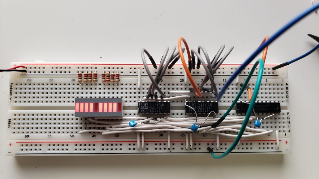
Now that I’ve arrived at the design requirements for a register in this processor, I can take the 74LS173 chips and add some additional hardware to make the whole thing work. Because I want to have readouts of the current register value, the register outputs have to be permanently enabled. That means I can’t rely on the ‘173s tristate output capability (tristate logic has a third state which is “high impedence”, essentially meaning that the line is disconnected from the circuit; this is useful for shared bus situations). Instead, the outputs can be permanently enabled and fed into a 74LS245 octal bus transceiver which is also connected to the ALU input bus. It may also make sense to put another 74LS245 on the input side of the register to reduce the number of devices directly connected to that bus. However, that is not included in this initial design.
I will create the register contents redout using an LED bar graph chip (10 segment, all independent) because I have some and the bar graph chips fit nicely onto a breadboard and take minimal space, unlike the complications of placing individual LEDs. This is easy enough since it will just have 8 LEDs connected to the 8 output lines of the ‘173s which will be active all the time anyway. These will, of course, be connected to ground with the usual current limiting resistors. The readout is, of course, optional, but it’s useful for debugging and also, who doesn’t like a bunch of blinkenlights. If you want to leave out the readout, you can also leave out the 74LS245 and instead connect the output enable input to the ‘173s directly.
With all that sorted, I now have a design for each general register. There will be several special purpose registers that I will get to later. That gives the schematic shown below.

Constructed on a breadboard, that gives the rat’s nest of wires in the picture below. Missing from the photo are the bus connections. The input connection will be on the left and the output connection on the right. You can see there is space on the left to add a ‘245 bus transceiver should it prove necessary. In the photo, the register has been loaded with decimal 255 (all bits set). As a variance from the schematic, I have left a space in the middle of the LEDs to group the bits in groups of four which makes it visually easier to read.
Exciting, isn’t it? Now I just need to build at least one more of those.